Open collector
Open collector output and open drain output utilize a transistor as a switch that either disconnects or connects an integrated circuit (IC) output pin to ground, instead of outputting a specific voltage or current.
Open collector

An open collector output processes an IC's output through the base of an internal NPN transistor, whose collector is an external output pin. The emitter of the NPN transistor is internally connected to ground.[1] The open collector internally forms either a short-circuit (technically low impedance or "low-Z") connection to ground when the transistor is switched on, or an open-circuit (technically high impedance or "hi-Z") when the transistor is off. The output is usually connected to an external pull-up resistor, which pulls the output voltage to the resistor's supply voltage when the transistor is off.
Analogous to open collector is the common emitter, which exposes the collector as the output while the emitter is connected to the negative voltage rail (NPN).
Open drain
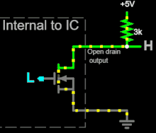
'Open drain output' is analogous to open collector operation, but uses a n-type MOS transistor (MOSFET) instead of an NPN.[1]: 488ff An open drain output connects to ground when a high voltage is applied to the MOSFET's gate, or presents a high impedance when a low voltage is applied to the gate. The voltage in this high impedance state would be floating (undefined) because the MOSFET is not conducting, which is why open drain outputs require a pull-up resistor connected to a positive voltage rail for producing a high output voltage.
Analogous to open drain is 'open source output', which exposes the MOSFET's source as the output while the drain is internally connected to the positive voltage rail.
Microelectronic devices using open drain output may provide a 'weak' (high-resistance, often on the order of 100 kΩ) internal pull-up resistor to connect the terminal in question to the positive power supply of the device so their output voltage doesn't float. Such weak pullups reduce power consumption due to their lower ohmic heating and possibly avoid the need for an external pull-up. External pullups may be 'stronger' (lower resistance, perhaps 3 kΩ) to reduce signal rise times (like with I²C) or to minimize noise (like on system RESET inputs).

Modern microcontrollers may allow programming particular output pins to use open drain instead of push–pull output, the strength of the internal pull-up, and allow disabling internal pullups when not desired.[2]
Schematic symbol

Open output is indicated on schematics with these IEEE symbols:[4]
- ⎐ - open collector or similar (e.g. open drain) pin that outputs a low voltage when on or hi-Z when off.
- ⎒ - variant with internal pull-up resistor to provide a high voltage when off.
- ⎏ - open emitter or similar (e.g. open source) pin that outputs a high voltage when on or hi-Z when off.
- ⎑ - variant with an internal pull-down resistor to provide a low voltage when off.
Applications
Note: since the name of this article is "open collector", this section primarily uses the term "open collector", however "open drain" generally applies as well.
Logic-level conversion
Because the pull-up resistor is external and does not need to be connected to the chip supply voltage, a lower or higher voltage than the chip supply voltage can be used instead (provided it does not exceed the absolute maximum rating of the chip's output). Open collector circuits are therefore sometimes used to interface different families of devices that have different operating voltage levels. The open collector transistor can be rated to withstand a higher voltage than the chip supply voltage. This technique is commonly used by logic circuits operating at 5 V or lower to drive higher voltage devices such as electric motors, LEDs in series,[5] 12 V relays, 50 V vacuum fluorescent displays, or Nixie tubes requiring more than 100 V.
Wired logic

Another advantage is that more than one open collector output can be connected to a single line. If all open collector outputs attached to a line are off (i.e. in the high-impedance state), the pull-up resistor will be the only device setting the line's voltage, and will pull the line voltage high. But if one or more open collector outputs attached to the line are on (i.e. conducting to ground), since any one of them are strong enough to overcome the pull-up resistor's limited ability to hold the voltage high, the line voltage will instead be pulled low. This wired logic connection has several uses.
By tying the output of several open collectors together and connecting to a pull-up resistor, the common line becomes a wired AND in active high logic. The output will be high (true) only when all gates are in the high impedance state and will be low (false) otherwise, like Boolean AND. When treated as active-low logic, this behaves like Boolean OR, since the output is low (true) when any input is low. See: Transistor–transistor logic § Open collector wired logic.
Line sharing
Line sharing is used for interrupts and buses (such as I²C or 1-Wire). Open collector output enables one active device to drive the shared line without interference from the other inactive devices. If push–pull output was mistakenly used instead, the active device attempting to set the line voltage low would be in competition with the other devices attempting to set the line voltage high, which would result in unpredictable output and heat.
SCSI-1 devices use open collector for electrical signaling.[6] SCSI-2 and SCSI-3 may use EIA-485.
Analog
Open collector outputs can also be useful for analog weighting, summing, limiting, digital-to-analog converters, etc., but such applications are not discussed here.
Disadvantages
One problem such open-collector and similar devices with a pull-up resistor is the resistor consumes power constantly while the output is low. Higher operating speeds require lower resistor values for faster pull-up, which consume even more power.
Also when driving a load, current through the pull-up resistor reduces the output high voltage by a voltage drop equal to the current times resistance, according to Ohm's law.
Open drain, drives high
Typically, open collector or open drain outputs connect to ground to represent low and disconnect to represent high. But by using a driving device of opposite polarity (PNP or P-channel), open collector or open drain outputs that drive high instead connect to the supply voltage to represent high and disconnect to represent low. GPIO pins can usually be configured for either polarity.
Pseudo open drain (POD)

Pseudo open drain (POD) drivers have a strong pull-down strength but a weaker pull-up strength. The purpose is to reduce the overall power demand compared to using both a strong pull-up and a strong pull-down.[7] A pure open drain driver, by comparison, has no pull-up strength except for leakage current: all the pull-up action is on the external termination resistor. This is why the term "pseudo" has to be used here: there is some pull-up on the driver side when output is at high state, the remaining pull-up strength is provided by parallel-terminating the receiver at the far end to the HIGH voltage, often using a switchable, on-die terminator instead of a separate resistor.
JEDEC standardized the terms POD15,[8] POD125,[9] POD135,[10] and POD12[11] for 1.5V, 1.25V, 1.35V, and 1.2V interface supply voltages, respectively.
DDR memory
DDR4 memory uses POD12 drivers but with the same driver strength (34 Ω/48 Ω) for pull-down (RonPd) and pull-up (RonPu). The term POD in DDR4 referring only for termination type that is only parallel pull-up without the pull-down termination at the far end. The reference point (VREF) for the input is not half-supply as was in DDR3 and may be higher. A comparison[12] of both DDR3 and DDR4 termination schemes in terms of skew, eye aperture and power consumption was published in late 2011.
See also
- Common collector and other common terminal transistor amplifiers: Used more for analog voltages than digital.
- Push–pull output: Consists of transistors to source and sink current in both logic states, not just one.
- Three-state logic: Consists of transistors to source and sink current in both logic states, as well as a control to turn off both transistors to isolate the output. This differs from open collector/drain output, which only use a single transistor that can only disconnect the output or connect it to ground.
References
- Paul Horowitz; Winfield Hill (1989). The Art of Electronics (2nd ed.). Cambridge University Press.
- Kotzian, Jiri (2015). "Influence of Pin Setting on System Function and Performance" (PDF). NXP. Archived (PDF) from the original on 2022-10-23. Retrieved 2022-12-27.
- "SNx407 and SNx417 Hex Buffers and Drivers With Open-Collector" (PDF). Texas Instruments. 1983. Retrieved 2023-01-18.
{{cite web}}: CS1 maint: url-status (link) - "Overview of IEEE Standard 91-1984 Explanation of Logic Symbols" (PDF). Texas Instruments. Texas Instruments. 1996. Retrieved February 12, 2020.
- Oskay, Windell (2012-02-29). "Basics: Open Collector Outputs". Evil Mad Scientist. Archived from the original on 2022-12-20. Retrieved 2023-01-15.
- "Overview of SCSI Standards & Cables". Archived from the original on 2008-12-10. 081214 scsita.org
- Addenddum No. 6 to JESD8 - High Speed Transceiver Logic (HSTL)- A 1.5 V Output Buffer Supply Voltage Based Interface Standard for Digital Integrated Circuits (August 1995).
- POD15 ‐ 1.5 V Pseudo Open Drain Interface (October 2009).
- Pseudo Open Drain Interface (September 2017).
- POD135 ‐ 1.35 V Pseudo Open Drain Interface (March 2018).
- POD12 ‐ 1.2 V Pseudo Open Drain Interface (August 2011).
- Pseudo-open drain and Center-tab termination type termination schemes